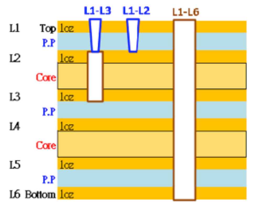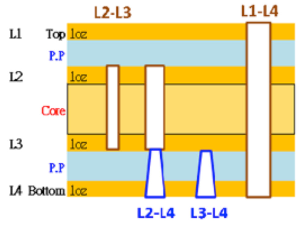
Parameter control for lamination four-layer board with finished thickness of 0.3mm.
Items requires lightweight, thin, and small size
Backplane bonding design to achieve a blind via effect.
Products with embedded component needs or special thickness requirements. For example: optical products, CMOS, RFID, and small-sized products.
Multi-layer board copper thickness: 6oz for inner layers / 6oz for outer layers.
Power-related boards or products with high-speed heat dissipation requirements.
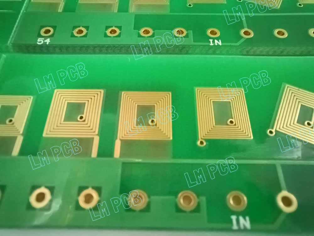
Inductor circuit board
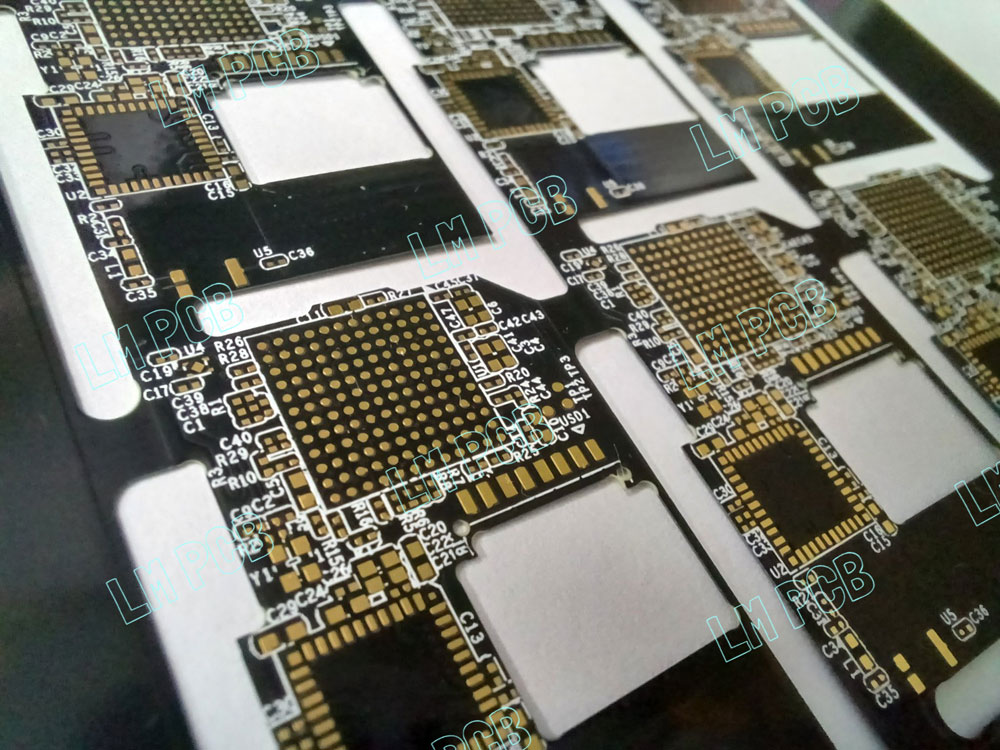
Wireless, communication devices, wireless charging devices.
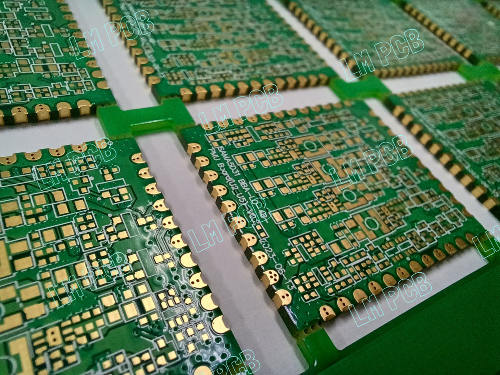
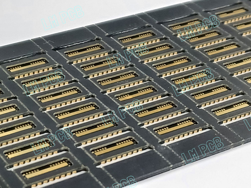
Through a special process, copper is plated on the half holes along the board edge.
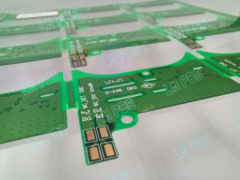
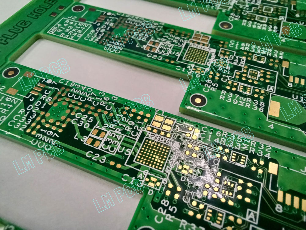
Functional requirements on the PCB edges (connection/welding) corresponding to specific products
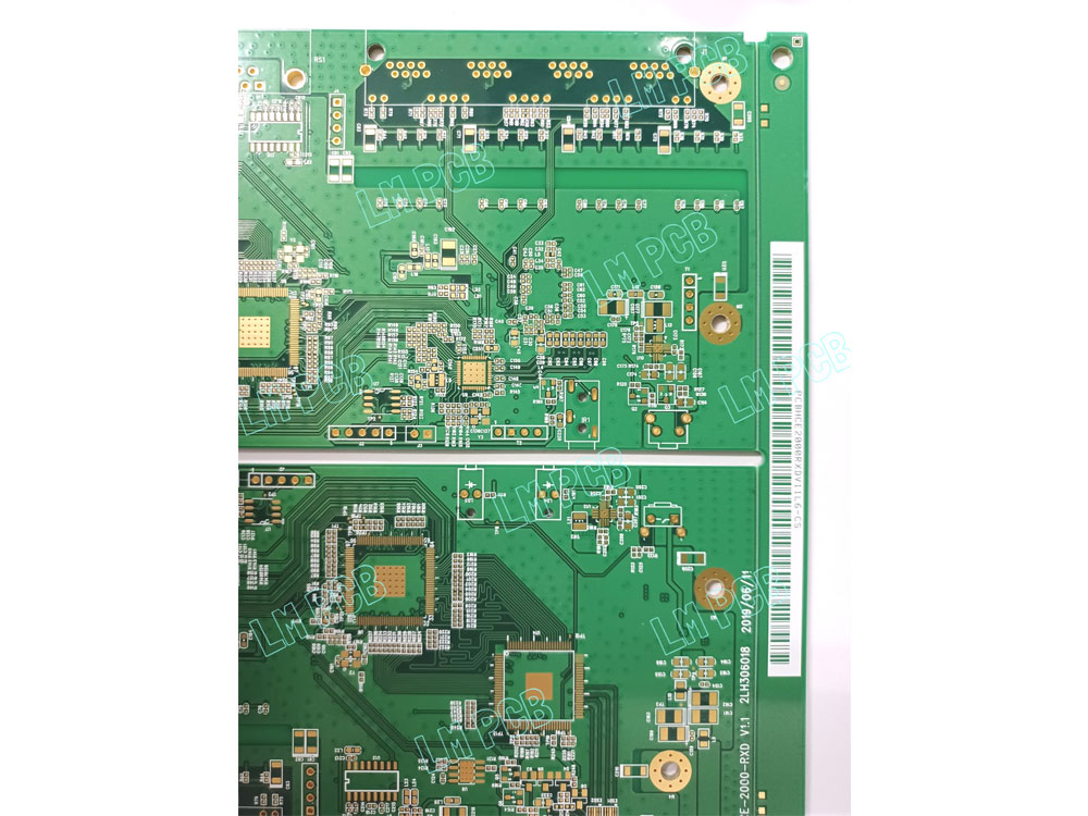
Flexible use of legend processes, printing customer part number,barcode on break edges (non-sequential number).
Barcode optimization for non-sequential products, saving customer labeling process time.
Requirements for composite SMD (Surface Mount Device).
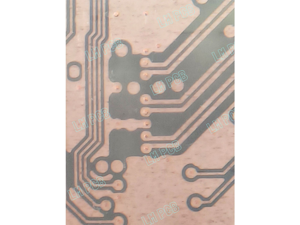
increase copper thickness according to PAD positions, forming a copper surface height difference (1~3oz) resembling copper columns, achieving cost reduction and improved heat dissipation.
Power-related, communication equipment, automotive equipment.
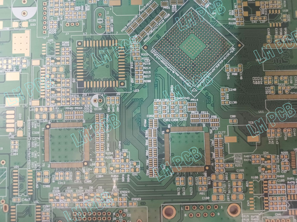
BGA routing with a pitch spacing of 0.4mm (without drilled holes).
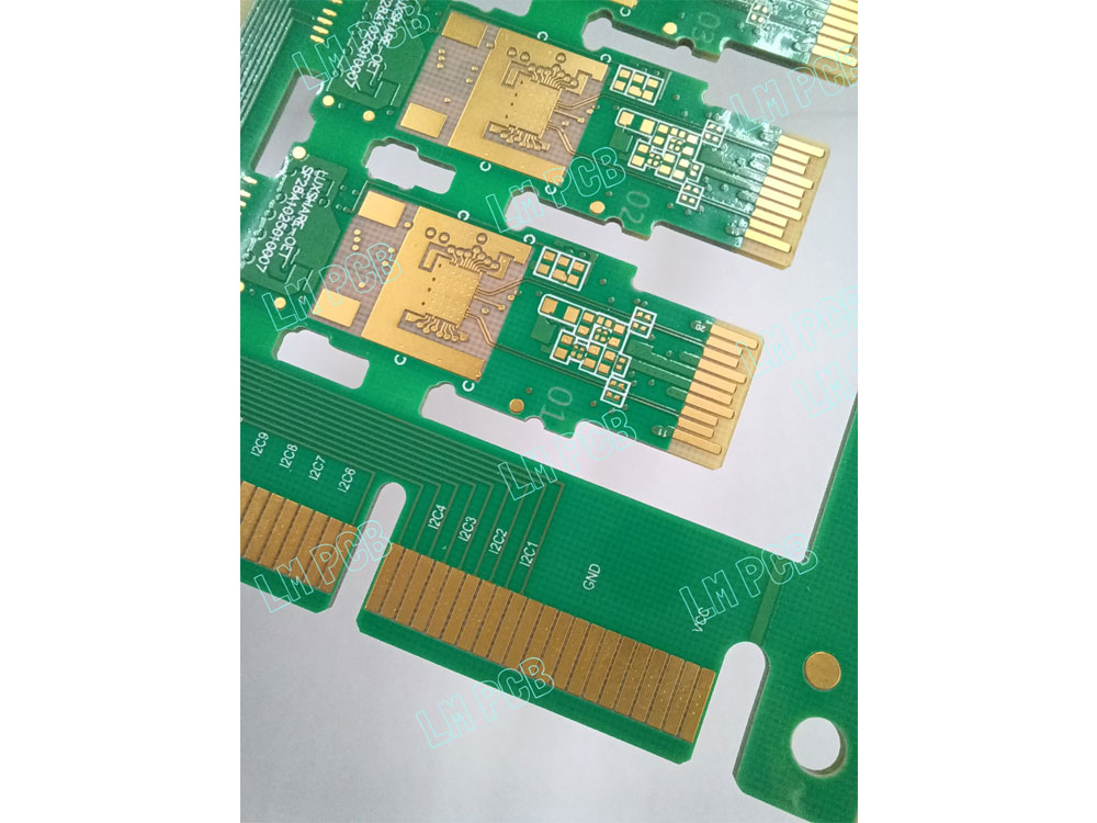
High-frequency substrate/gold fingers (G/F tip w/o conductive wire ).
High-frequency products, 50G, 100G+, high transmission speed products. Example industries: optical fiber, communication, automotive.
Double-sided PCB - finished thickness of 0.18mm.
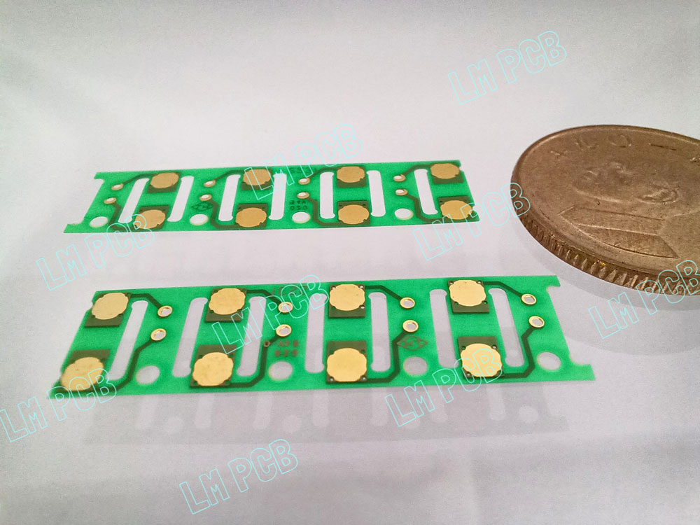
Product application: Medical equipment - blood glucose meters.
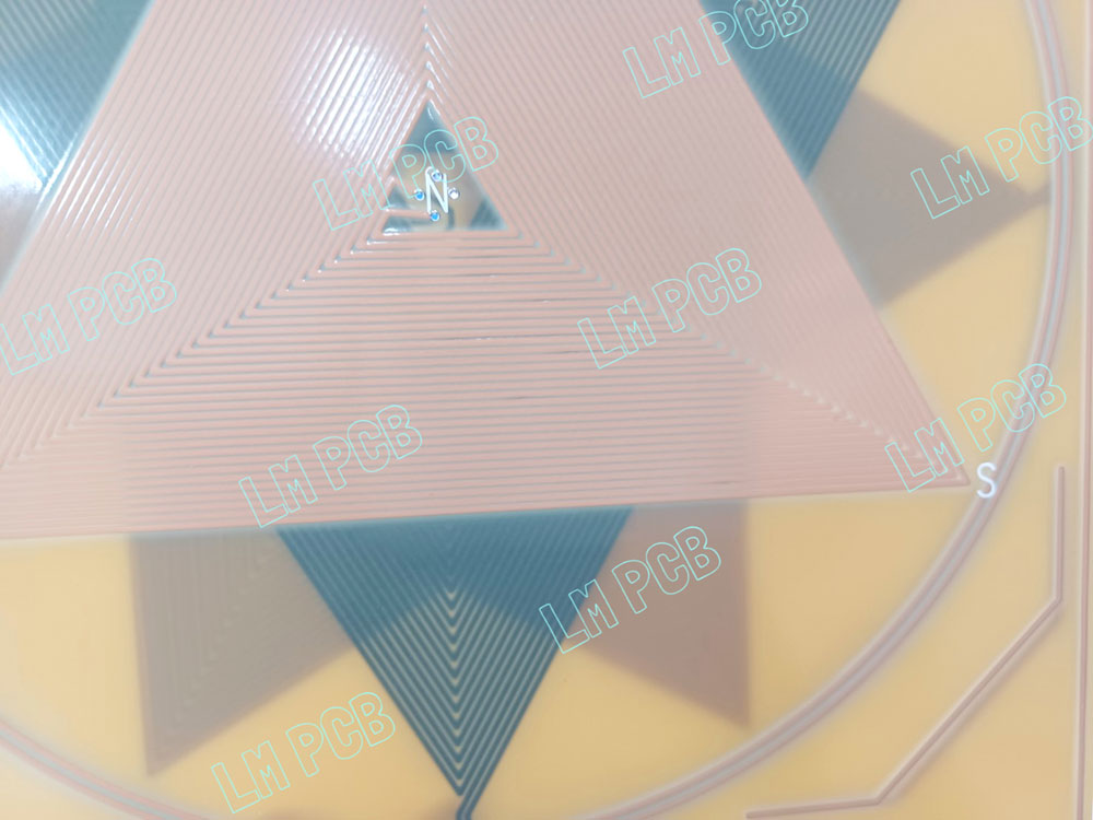
Inner layers: 4oz / Outer layers: 4oz / Inductor design / Transparent solder mask.
Product application: Network communication - resonators.
Double-sided board - finished thickness of 0.2mm.
SD cards, wearable products.